Silicon Is Reaching Its Limits. Up Next: Carbon Nanotubes

Share
Silicon has powered the information age, but it’s reaching its physical limits. Carbon nanotubes (CNTs) hold a lot of promise as a replacement if we can get around some key obstacles—and the designers of a new chip seem to have done just that.
For decades computer power steadily increased in line with Moore’s Law, which observed that the number of transistors in a chip doubled roughly every two years. That was made possible by the progressive shrinking of these transistors, but as they approach the scale of a few tens of atoms there’s been a marked slowing in this trend.
That’s prompted a search for a successor to the traditional silicon chip that’s boosted research in areas like optical computing, brain-inspired neuromorphic chips, and processors made from exotic new materials.
One of the more promising candidates is chips made from CNTs, which have several attributes that should make for high-performance, energy-efficient processors. These tiny tubes of atomically thin carbon sheets are just nanometers in size, transport charge carriers very quickly, and are also excellent semiconductors, which means they can both conduct electricity and shut it off just like silicon.
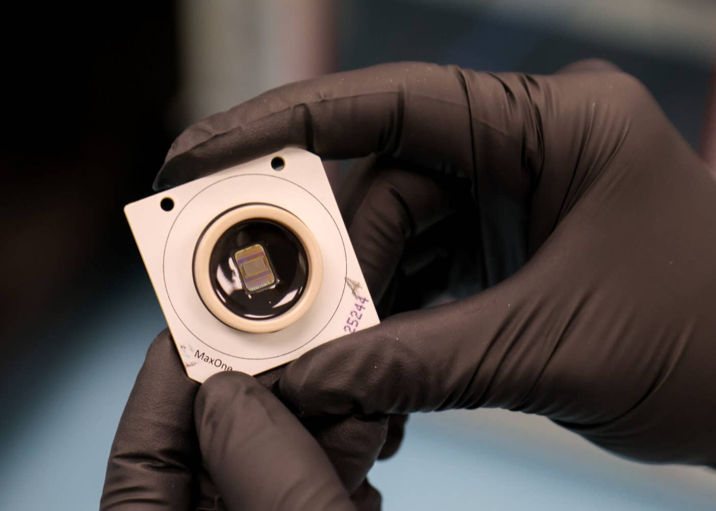
IBM made the first CNT transistors two decades ago, but attempts to create large-scale processors using CNTs have so far been plagued by fabrication and purity problems. Now scientists have demonstrated a 16-bit microprocessor built from over 14,000 CNT transistors that successfully executed a program that produces the message “Hello, World! I am RV16XNano, made from CNTs.”
While 16-bits is still small, it’s a big leap from the 1-bit, 178 transistor that project leader Max Shulaker built with other researchers in 2013. And more importantly, the chip described in a recent paper in Nature was built using industry-standard design processes, suggesting the technique could potentially be scaled up to commercial production.
That’s crucial for the group’s funder, DARPA, which invested $61 million in the project last year as part of its Electronics Resurgence Initiative. The project’s goal is to manufacture 3-D stacked carbon nanotube circuits in a commercial semiconductor factory.
The high temperatures used to fabricate silicon mean it’s not possible to layer circuits on top of each other, but the lower processing temperatures used to process CNTs should make it feasible. Taking circuits into the third dimension could let designers squeeze much more computing power into chips.
Getting round the obstacles that had stymied previous attempts at CNT chips required some inventive thinking, though. The biggest issue is purity; the process for making CNTs is not flawless, and a small fraction end up with defects that make them act like a fully conductive metal rather than a semiconductor.
Too many of these metallic CNTs can slow or stop a transistor’s ability to switch from on to off, the process at the heart of binary logic. The researchers calculated it would take a purity of 99.999999 percent to avoid this outcome, but current processes only yield purities of 99.99 percent.
The key to getting round this was the realization that different combinations of logic gates—groups of transistors designed to carry out a specific operation—were more susceptible to metallic CNTs than others. That led the team to create a set of design rules that avoid vulnerable combinations, allowing them to still build functional circuits at 99.99 percent purity.
Be Part of the Future
Sign up to receive top stories about groundbreaking technologies and visionary thinkers from SingularityHub.


Another problem they had to work around was the tendency of CNTs to bundle together when applied to the silicon wafer supporting the circuit, which leads to large clumps that can’t form transistors. The group created an exfoliation process that essentially washes away these big bundles.
The final breakthrough was a method for reliably creating the two essential transistor types: “N” types, which turn on when they receive 1 as an input and off when they receive 0, and “P” types, which do the opposite. Making both types with CNTs has been tricky, and previous chips have consisted solely of P type transistors. But the researchers came up with a way to fix the transistors with different metals to reliably determine their type.
The group is now working to implement their manufacturing techniques at a silicon chip foundry, and Shulaker thinks commercial products could be less than five years away. In a commentary accompanying the paper in Nature, Franz Kreupl from the Technical University of Munich suggests there may still be some way to go, though.
While the research overcomes major obstacles to creating a functional CNT processor, making one that’s actually useful requires further work, he writes. The new chip is comparable to Intel’s 80386 processor built in 1985, but while that could operate at a frequency of 16 megahertz, the new CNT chip runs at just 1MHz.
That’s because the speed at which you can switch transistors depends on how much charge its components can store, and the CNT transistors used in the new chip can hold only a fraction of that of silicon ones.
Kreupl suggests several ways this could be boosted from reducing the length and width of the CNTs and boosting their density, but adds that future large-scale CNT computers will need transistors with just a single nanotube that will have to be reliably semiconducting. That suggests the group’s design-based workaround may have its limits, and hitting the stringent purity requirements may still be necessary.
“The authors’ work is a great accomplishment that touches on many research topics—from materials science to processing technology, and from circuit design to electrical testing,” writes Kreupl. “However, more effort is required before the team will need a sales department.”
Image Credit: Felice Frankel, MIT / CC BY-NC-ND 3.0
Related Articles

US Issues Grand Challenge: The First Fault-Tolerant Quantum Computer by 2028

These Mini Brains Just Learned to Solve a Classic Engineering Problem

Brain Implants Let Paralyzed People Type Nearly as Fast as Smartphone Users
What we’re reading
