IBM’s New Chip Technology Shows Off the Next Big Step in Moore’s Law
Share
Increasingly, modern life depends on how skillfully we shuttle electrons through the nanoscale mazes etched on computer chips. These processors aren’t just for laptops anymore—they’re used in your car, your thermostat, your refrigerator and microwave.
And the pandemic has revealed just how deeply our dependence runs.
A global shortage of computer chips, brought on by vacillating demand and supply chain issues, is currently rippling through device-makers, of course, but also makers of cars, vacuum cleaners, and stove vents.
Clearly, we’re hooked.
So, perhaps it’s no surprise that when companies announce better, faster, more efficient computer chips, the world takes notice. This week, it was IBM’s turn to make headlines.
The company, once synonymous with all things computing, announced that it’s demonstrated a 2-nanometer (nm) chipmaking process for the first time.
In a press release, IBM said the new process would yield some 50 billion transistors on a chip the size of a fingernail. It would also bring chips that are 75 percent more efficient or 45 percent faster than today’s 7-nm chips.
On its face, it would seem IBM just leapt far ahead in the race for top chip tech. Intel’s latest chips use a 10-nm process and TSMC’s use a 7-nm process. And the company has made some very cool and notable progress here. But comparing chips is complicated. So, it’s worth dissecting the news a bit more to better understand the bigger picture.
Nanometer to Nanometer Is Apples to Oranges
Progress in computer chips has long been measured in nanometer-sized steps. Each step down yields ever more components—most notably, transistors—packed into the same area. And there was a time, in decades past, when the nanometer nomenclature actually did match the size of certain chip elements. But that time has passed. As chip technology advanced, the measurements of chip components decoupled from each generation’s naming convention.
By the time chips made the last big leap to FinFET—a 3D transistor design shaped like a fin—a little over a decade ago, the industry’s node number was virtually meaningless. It didn’t relate to any dimension on the chip. There’s currently a debate over what new number, or combination of numbers, better reflects progress. And although this too is proving rather complicated, one spec experts propose is transistor density per square millimeter.
To see how the old naming convention is confusing, compare Intel’s 10-nm chips with TSMC’s 7-nm chips. The two actually have roughly equivalent transistor densities, with Intel’s 100 million transistors per square millimeter actually edging out TSMC’s 91 million per square millimeter. (Go here for a handy table comparing process size and transistor density of chips.)
IBM didn’t announce transistor density explicitly. But after reaching out to clarify exactly what sized “fingernail” they were referencing—representatives of the company said about 150 square millimeters—the publication AnandTech calculated IBM’s new process would yield some 333 million transistors per square millimeter. Which is, indeed, beyond anything in production. That said, a 3-nm chip TSMC is making for Apple could boast almost 300 million transistors per square millimeter and enter production as soon as next year.
Nanosheets: The Next Step in Moore’s Law?
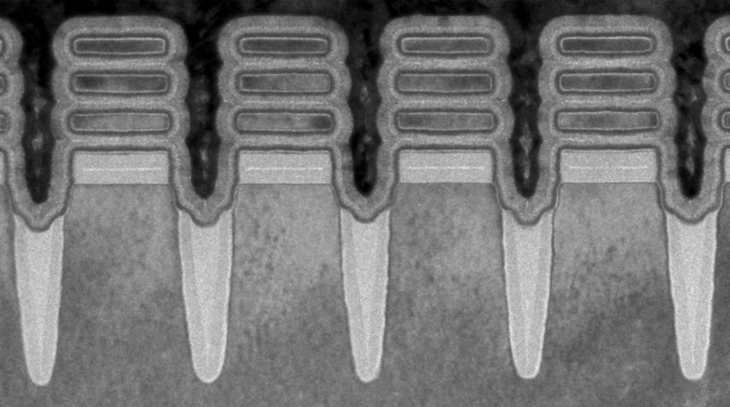
Perhaps the more significant news is the design of the transistors themselves. IBM's new technology—called nanosheet or gate-all-around transistors—is the long-awaited successor to today’s FinFET transistors. The company has been working on the tech since 2017.
FinFET transistors consist of a fin-shaped channel surrounded on three sides by a “gate” that controls the flow of electrons. But IBM's nanosheet (or gate-all-around) transistors have a layered channel instead. The layers are stacked on top of each other and, like three pigs-in-a-blanket, are surrounded by the gate on all sides. This last bit is the most critical piece. Gate-all-around transistors provide better control of current through the channel, prevent leakage, and boost efficiency.
Be Part of the Future
Sign up to receive top stories about groundbreaking technologies and visionary thinkers from SingularityHub.

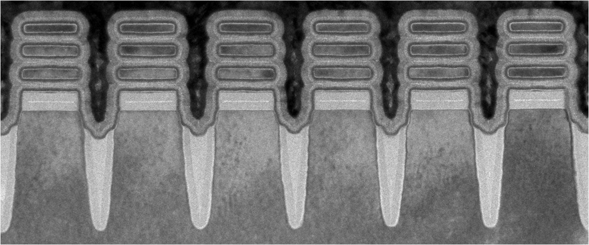
Nanosheet transistors fabricated using IBM's new 2-nanometer process. Image Credit: IBM
“It’s a tremendously exciting technology,” Jesús del Alamo, a professor at MIT who specializes in novel transistor technologies, told Wired. “It’s a completely new design that pushes forward the roadmap for the future.” And while IBM may be the first to show the tech off at this level, they likely won’t be the last. Samsung and TSMC will probably follow suit.
It’s too early to make serious performance comparisons between today’s production chips and future chips using IBM’s new transistors, but it's safe to say they'll offer notable improvements. Dan Hutcheson, CEO of analytics company VLSI Research, told Wired IBM’s estimated performance improvements actually seemed conservative and called the work a “milestone for the industry.”
Next-Generation Chips
When might you buy a device with one of these chips? Likely not for a bit.
Though IBM still designs chips, it sold its chipmaking business in 2014. This new tech hails from its research facility in Albany, New York and is a demonstrator, not a production-ready chip. In the coming years, IBM will complete the process, at which point it may make its way into production chips by way of licensing deals with partners like Intel and Samsung.
The industry isn't likely to stand still in the interim. There's a renaissance of sorts in the chip industry right now.
It's no longer only about spending billions to wring a few more drops from traditional chips. There's energy and innovation reinvigorating the sector and bringing about a Cambrian explosion of bizarre designs for special purposes, like AI. And much of it is taking place outside big companies.
For the first time in years, venture capital is pouring into startups—more than $12 billion, in fact, went to over 400 chip companies in 2020 alone.
So, even amid this year's chip drought, it seems the monsoon is gathering.
Image Credit: IBM

Jason is editorial director at SingularityHub. He researched and wrote about finance and economics before moving on to science and technology. He's curious about pretty much everything, but especially loves learning about and sharing big ideas and advances in artificial intelligence, computing, robotics, biotech, neuroscience, and space.
Related Articles

Orbital Data Centers Are Seductive on Paper, but They Face Daunting Challenges in Reality

In the Scramble to Power AI, Investors Bet $140 Million on Data Centers at Sea

Quantum Computers Are Coming to Break Cryptography Faster Than Anyone Expected
Orbital Data Centers Are Seductive on Paper, but They Face Daunting Challenges in Reality
In the Scramble to Power AI, Investors Bet $140 Million on Data Centers at Sea
Quantum Computers Are Coming to Break Cryptography Faster Than Anyone Expected
What we’re reading