IBM Creates Nano-sized 3D Map of Earth in Less Than 3 Minutes! (Video)
Share
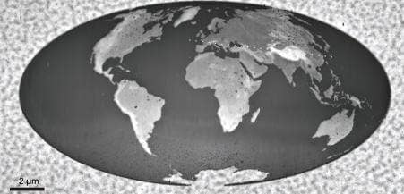
What do you do after 20 years of leading the world in microscopy? Apparently you show off a little. IBM recently unveiled the latest in its micro-scale techniques - a nanoscale system capable of ultra-precise and rapid lithography. To demonstrate the system's prowess they scratched out a relief map of the Earth that was only 22 by 11 microns. One thousand of these maps could fit on a single grain of sand. Even more impressive, the map took less than three minutes to complete but was made to scale (1000 meters of elevation = 8 nanometers of depth on the map)! This and related work was recently published in Science and Advanced Materials. IBM's new technique could allow for the cheap and rapid production of nanoscale creations with applications in computing and material sciences. Check out IBM's explanation for their incredible feat in the video below, the map appears around 1:25.
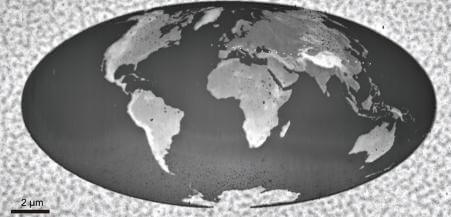
Last year IBM revealed the first true images of a molecule using a special atomic force microscope (AFM) with a carbon monoxide tip. AFMs have been around for a while, but IBM continues to find interesting ways to innovate them. The nanoscale 3D map was created using an adapted AFM setup that allowed a very small (few nanometers) silicon tip on the end of a cantilever to be heated as it brushed against a special polymer surface (polyphthalaldehyde). Essentially the tip carved this polymer to create the relief map of the globe. IBM also created a replica of the Matterhorn on a molecular glass substrate using the same technique. In both cases, the AFM-like tip was used to not only create the image, but also to "view" the image when it was completed.
Be Part of the Future
Sign up to receive top stories about groundbreaking technologies and visionary thinkers from SingularityHub.

As the video mentions (vaguely), this isn't the most precise nano-sized endeavor ever attempted. Scientists routinely work on submicron scales to create all manner of nanodevices, including lasers. Heck we've even seen a snowman that was similar in size to IBM's nano-maps. Yet, as IBM points out in the Advanced Materials article, it isn't enough to simply construct an interesting nanoscale creation. For a real-world application you need to handle a large volume of such microscopic tasks without having your microscopic equipment break down. That's why IBM's system represents a real break through. Their silicon tip is sturdy, and can handle a large workload. IBM's essentially created a rapid nanometer scale lithography system. Their new AFM-like tip for scratching, and the use of polymer and glass surfaces as substrates, allows them to quickly construct nanometer paths. What others can do at the same scale, IBM is attempting to do faster, easier, and cheaper.
Those nanometer paths could allow all manner of new creations. They may be used to facilitate the assembly of nanomaterials by helping molecules move in the right directions. They could serve as a pattern for printing pathways on other surfaces. Or, if the substrates have the right properties, they may even be used to create actual electrical or opto-electrical devices. All of this and they should be able to be made quickly, reliably, and in manufacturing conditions.
Certainly part of the reason companies like IBM go to the trouble of creating stunning displays of their microscopic prowess is to demonstrate the efficacy of their new techniques. But just as importantly, it serves as a place holder in the public mind while the company works on developing real applications for that technique. It is likely to take many years for IBM to design some sort of product that is created using their newest AFM/silicon tip method. It will be years after that until they go ahead and produce such an item and we have a chance to buy it. In the meantime, the incredibly tiny map serves as a good indication of the remarkable potential for their technique.
[image credit: Advanced Materials]
[video credit: IBM]
[sources: IBM, Science, Advanced Materials]
Related Articles

Orbital Data Centers Are Seductive on Paper, but They Face Daunting Challenges in Reality

In the Scramble to Power AI, Investors Bet $140 Million on Data Centers at Sea

Quantum Computers Are Coming to Break Cryptography Faster Than Anyone Expected
Orbital Data Centers Are Seductive on Paper, but They Face Daunting Challenges in Reality
In the Scramble to Power AI, Investors Bet $140 Million on Data Centers at Sea
Quantum Computers Are Coming to Break Cryptography Faster Than Anyone Expected
What we’re reading