New Photonic Synapses Mimic the Brain and Compute With Light

Share
Computing with light and designing brain-inspired hardware are at the experimental fringes of technology research. But they both come with potentially enormous advantages, so a group of scientists has decided to combine them.
Neuromorphic computing attempts to mimic the hardware of biological brains to harness their ability to carry out complex calculations on a fraction of the energy conventional computers require. Most attempts so far have sought to build these devices using the same electronic components at the heart of their classical counterparts.
In recent years though, some researchers have turned to photonics—a field focused on manipulating the photons that make up light to carry out communication and computing tasks in similar ways to how electronics uses electrons.
A key step for neuromorphic computers is creating components analogous to the brain’s network of neurons and the connections between them called synapses. Now, scientists from the UK and Germany have created a photonic synapse that mimics crucial characteristics of its biological counterparts while harnessing the speed and energy-efficiency of photonic computing.
"We've demonstrated the world's first integrated photonic synapse,” says Zengguang Cheng, a postdoctoral fellow at the University of Oxford and lead author of a paper describing the advance in Science Advances.
“We believe this is a crucial step for optical brain-inspired computing. It combines neuromorphic computing with photonic computing and brings all of their advantages together.”
The researchers built their artificial synapse by integrating a phase-change material (PCM) commonly used in rewritable CDs and DVDs onto a waveguide—the photonic equivalent of a wire used to transport photons.
The PCM’s ability to absorb light changes when heated, which can be used to control the amount of light that passes through the waveguide. In previous research, the group had shown that optical pulses could be used to switch between various states of absorption to store information—effectively creating a photonic memory device.
The synapse is effectively the brain’s memory device, storing information in the strength of connections between neurons. This made the PCM-based photonic memory a good starting point for the researchers, but switching between states required complicated arrangements of optical pulses at different powers.
To simplify the system, the researchers wanted to control it with pulses with fixed characteristics. So rather than using a single chunk of PCM attached to a standard waveguide, they tapered the central section of their waveguide and used six separate PCM islands.
This allowed the optical pulses to disperse more uniformly through the device, which gave the researchers greater control when switching between the PCM’s various states. This made it possible to shift between 11 distinct synaptic weights using fixed numbers of optical pulses of the same power and duration.
They predict they will be able to optimize the design to get many more synaptic weights, possibly even approaching the continuous, analog weighting seen in biological synapses.
Despite the similarities to a biological synapse though, there is one key difference. The strength of connections in the brain depends on the timing of the firing of neurons either side of the synapse via a rule called spike-timing-dependent plasticity (STDP) that is at the heart of learning and memory formation.
The weight of the photonic synapse is governed by the number of pulses instead. Fortunately, says Cheng, both of these relationships are exponential, which means it’s relatively simple to set up a photonic circuit so that the time delay in the neuron signals correlate with the number of pulses. They do this in their paper, thereby replicating the STDP rule in a photonic circuit.
Be Part of the Future
Sign up to receive top stories about groundbreaking technologies and visionary thinkers from SingularityHub.


“This design constitutes a significant step forward in terms of programmability, allowing the control of synaptic weights with standardized optical pulses,” Cesare Soci , an associate professor at Nanyang Technological University, Singapore, who has worked on photonic synapses.
“Integrated optical waveguides will also facilitate cascadability and fan-out, which will be essential to scale up neuromorphic computing chips with billions of photonic synapses, operating at powers comparable to the brain.”
Qiangfei Xia, an associate professor at the University of Massachusetts who works on electronic approaches to neuromorphic computing, said the photonic synapse is a smart idea and could significantly reduce power consumption. He did point out though that both the synapse and the waveguides are relatively large compared to electronic components.
“It remains to be demonstrated how densely the photonic synapses can be packed into large arrays for neuromorphic computing purposes,” he added.
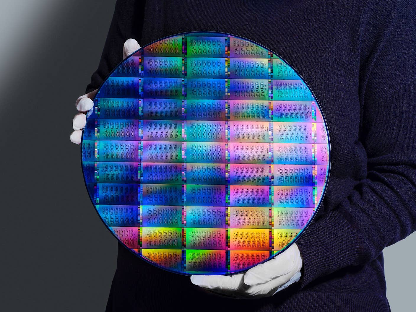
That is the ultimate goal for Cheng and his colleagues. Their fabrication technique is compatible with traditional chip-making processes, and to demonstrate its scalability, they built a roughly 1 centimeter-long chip containing 70 of the photonic synapses.
Before they can put them to use though, they first need to create a photonic neuron to wire them together. That’s a considerably trickier challenge says Cheng.
"Definitely the neuron is more complex,” he adds. “We can think about the synapse as just a memory unit, but the neuron cell body can be thought of as a discrete CPU implementing algorithms, so it's definitely more complicated.”
But they’ve had some promising results so far, he says, and they hope to publish their progress early next year—so, watch this space.
Image Credit: Gwoeii / Shutterstock.com
Related Articles

Quantum Computers Are Coming to Break Cryptography Faster Than Anyone Expected

Printed Neurons That Mimic Brain Cells Could Slash AI’s Energy Bill

Scientists Grow Electronics Inside the Brains of Living Mice
What we’re reading
