How Scientists Squeezed a Particle Accelerator Onto a Tiny Silicon Chip

Share
Particle accelerators have helped us unravel some of the universe’s biggest mysteries, but they're huge, expensive, and inaccessible to most researchers. A new particle accelerator on a chip could soon change that.
The world’s biggest particle accelerators can be miles long and require megawatts of power to run. Even devices used to generate particle beams for medical therapies can be the size of a room. So in 2015, the Gordon and Betty Moore Foundation awarded Stanford University $13.5 million to build a particle accelerator the size of a shoebox and put these crucial scientific and industrial tools in the hands of far more scientists.
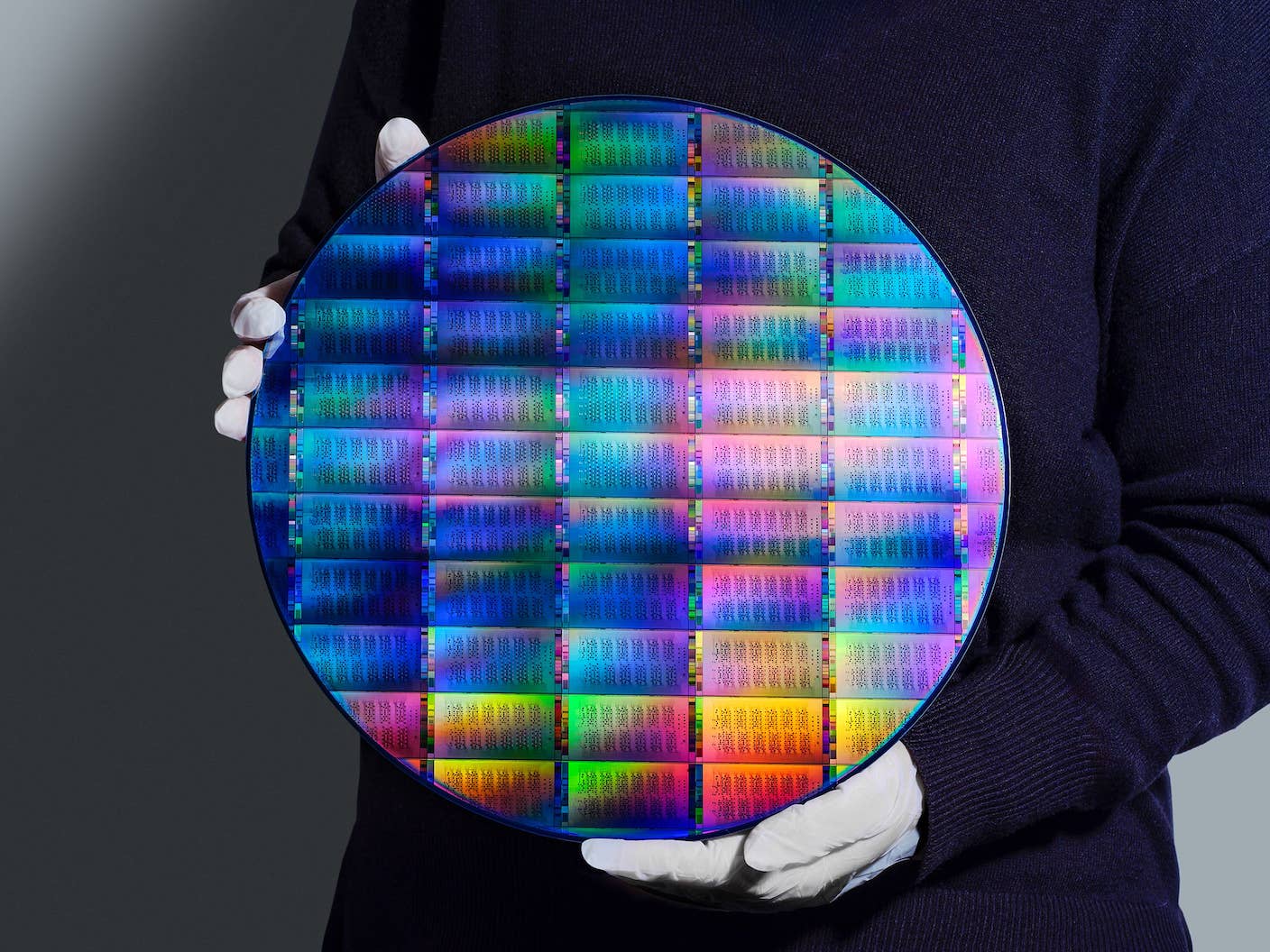
Now, researchers have developed a tiny silicon chip smaller than the width of a human hair that can accelerate electrons using an infrared laser. The output is only a fraction of that of a large accelerator, but the researchers plan to combine a thousand of these devices by the end of this year to accelerate electrons to 94 percent of the speed of light, or 1 million electron volts (1MeV), which would be powerful enough for research or medical purposes.
"The largest accelerators are like powerful telescopes. There are only a few in the world and scientists must come to places like SLAC [the Stanford Linear Accelerator] to use them," Jelena Vuckovic, who led the research, said in a press release. "We want to miniaturize accelerator technology in a way that makes it a more accessible research tool."
Accelerators typically use microwaves to push particles ever faster, but these have wavelengths on the order of several inches, which restricts how small the machines can be made. The new device, described in a paper in Science, uses pulses of infrared laser light instead, which have wavelengths on the order of a micrometer and therefore can accelerate the particles over much shorter distances, significantly reducing size requirements.
Designing devices at these tiny scales is much harder, so the researchers developed a special “inverse design” algorithm. They specified what they were trying to achieve and the software then automatically suggested a nanoscale structure that could effectively channel the laser photons to the electrons and give them a speed boost.
“If you look at the design, no human engineer would have come up with it,” lead author Neil Sapra told Vice. “I really don’t think I could have done this project without this inverse-design technique because coming up with a design is pretty difficult doing the classical approach.”
The computer-designed layout was then carved into silicon and sealed in a vacuum to create a channel through which electrons could be beamed. Silicon is transparent to infrared light, so when an on-chip laser fires pulses at the structure it’s transmitted through the walls, creating an electric field that accelerates the electrons.
Be Part of the Future
Sign up to receive top stories about groundbreaking technologies and visionary thinkers from SingularityHub.


A single stage can currently boost the speed of the electrons up to 1KeV (a thousandth of a MeV), but because the device is an integrated circuit it shouldn’t be too complicated to stitch many of the devices together to accelerate them to much higher energies. They are fabricated using industrial processes, which should allow for significant cost reductions.
If the team achieves their goal, the resulting device could make it possible for far more scientists to carry out cutting-edge experiments in chemistry, materials science, and biological discovery.
One particularly promising application would be to use them to create small bunches of electrons that result in x-ray pulses just a few attoseconds (one quintillionth of a second) long. These could be used to probe chemical reactions and other events at the molecular scale on extremely short timescales to create “molecular movies," Joel England, one of the authors of the paper, told IEEE Spectrum in 2017.
There could also be promising medical applications of the technology. One of the authors is working on a way to transport high-energy electrons from the accelerator-on-a-chip directly to tumors using a catheter-like vacuum tube that could be inserted below the skin. That would be a major improvement over today’s bulky and tricky-to-focus X-ray based radiotherapy devices.
The device is probably a long way from replacing the massive accelerators used for particle physics experiments. But the researchers point out that computers have shown that stitching together thousands of low-cost integrated silicon chips is an incredibly powerful and scalable design approach. So never say never.
Image Credit: Image by Gerd Altmann from Pixabay
Related Articles

Quantum Computers Are Coming to Break Cryptography Faster Than Anyone Expected

Printed Neurons That Mimic Brain Cells Could Slash AI’s Energy Bill

Scientists Grow Electronics Inside the Brains of Living Mice
What we’re reading
